See Full Size
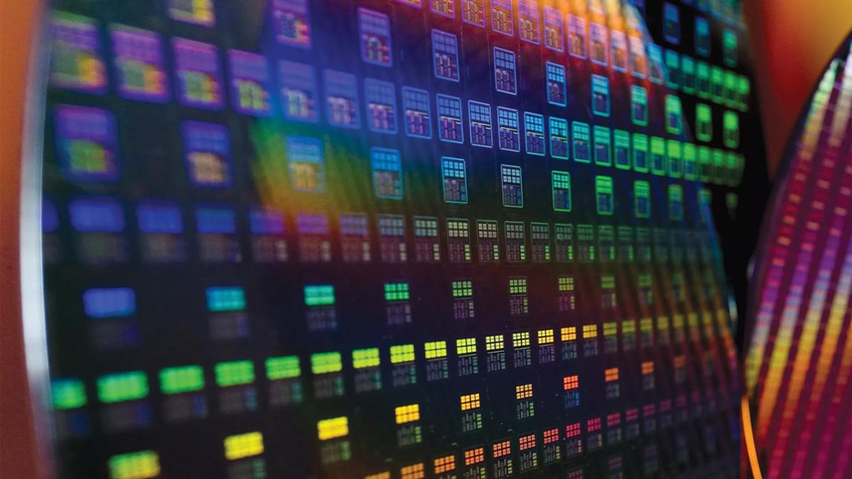
In the presentation made at the IEEE International Electronic Devices Meeting (IEDM) in San Francisco, TSMC said, “nanosheet” N2 technology based on transistors came to the fore. TSMC’s 2nm (N2) technology represents the company’s first attempt with nanosheet architecture, also known as “gate-all-around” (GAA).
There is serious progress in every field
See Full Size
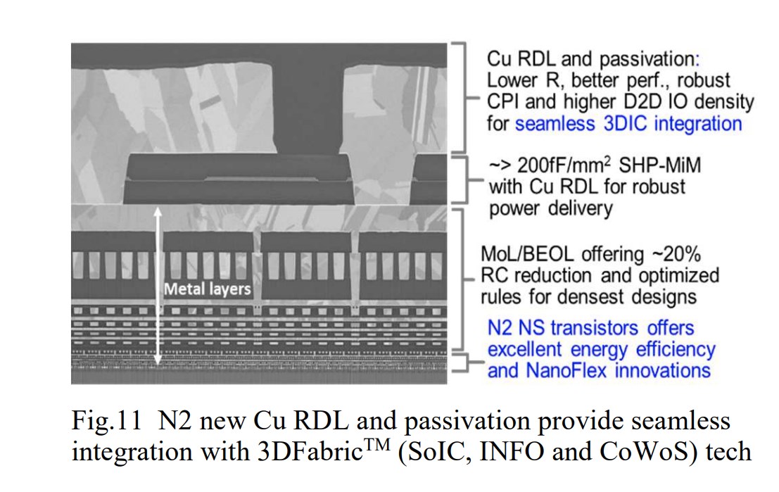
TSMC is shifting from traditional FinFET technology to nanosheet-based N2, gaining greater control over current control. Unlike FinFET technology, nanosheet transistors are created by stacking silicon into narrow strips. This design provides much more precise control than FinFET and allows manufacturers to customize process parameters according to use cases.
See Full Size
Prices are increasing
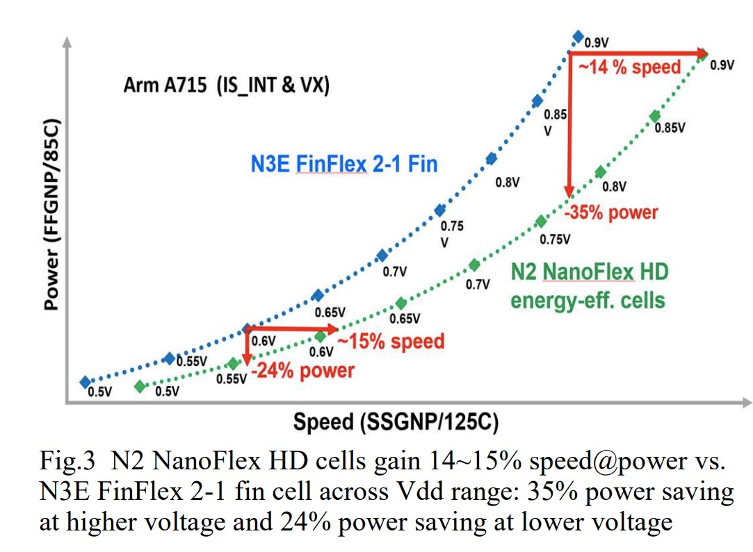
These developments are expected to be adopted by industry giants, especially Apple and Nvidia. It is stated that the new generation 2nm technology offers significant advantages compared to the previous 3nm process. However, as with every technological advance, they also have a cost. TSMC predicts that wafer prices for the N2 process will increase by more than 10 percent, to between $25,000 and $30,000. In the 3nm process, this figure was around $20,000.
It is estimated that adaptation will be slow due to low yield rates and trial production in the initial production stages of the new process. However, it is thought that high performance and energy efficiency advantages will offset these costs in the long run.
The race will be tough
See Full Size
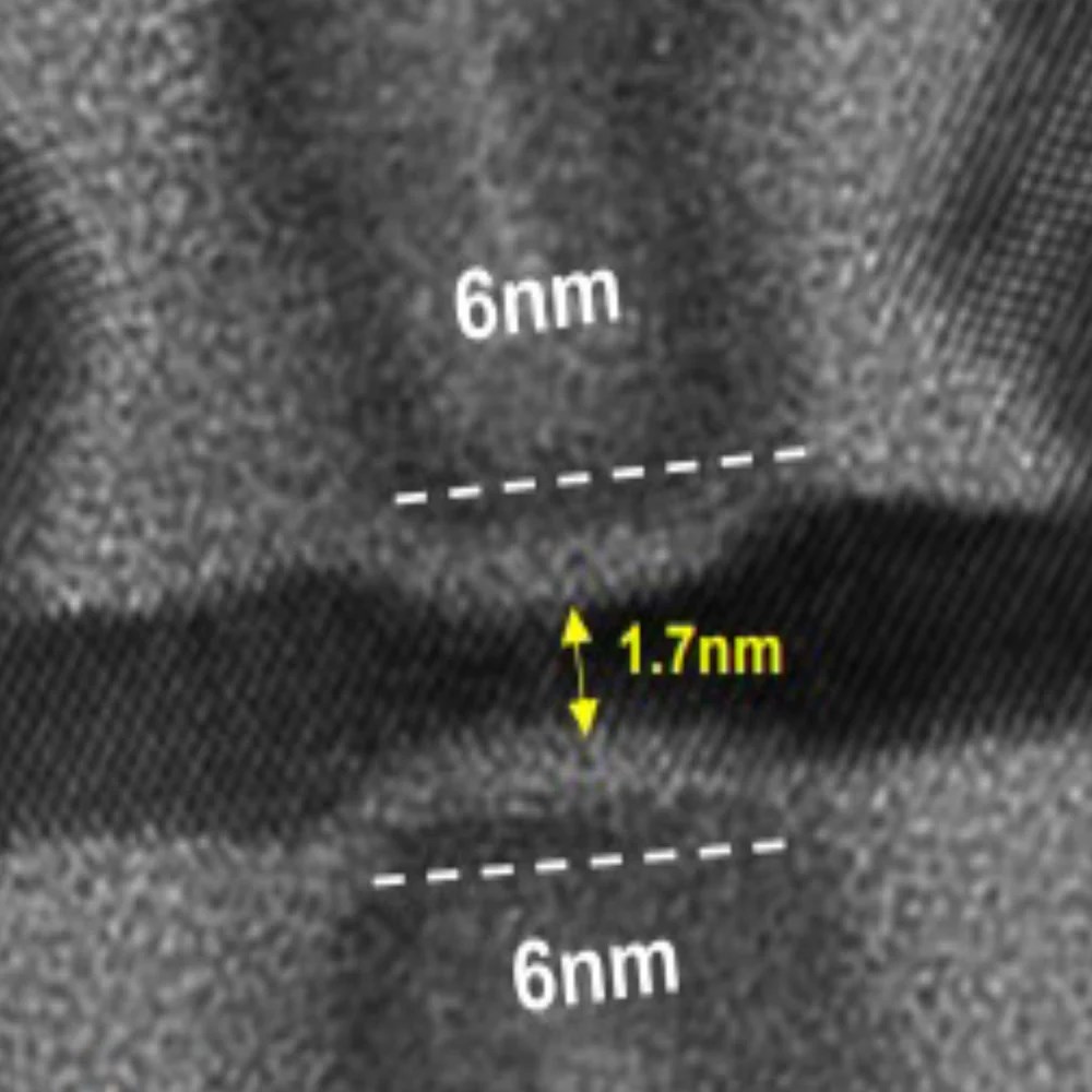
It is stated that there is currently no blockage in Intel’s silicon-based nanosheet architecture. “We haven’t hit the wall. It can be done, and here’s the proof,” said Sanjay Natarajan, vice president of Intel Foundry, emphasizing that current technology still has the potential to advance.
Samsung, Intel ve TSMCof nanosheet in 2025 Considering that it plans to start production with its technology, it is clear that intense competition is at the door in the semiconductor industry. While TSMC’s N2 technology raises the bar in the industry in terms of performance and energy efficiency, Intel’s future studies reveal the long-term potential of this technology.
Source
https://wccftech.com/tsmc-details-its-high-end-2nm-process-revealing-performance-efficiency-improvements/
https://spectrum.ieee.org/tsmc-n2
This news our mobile application Download using
You can read it whenever you want (even offline):


