See Full Size
High demand for glass substrate technology
Besides AMD Intel ve Samsung Leading chip manufacturers such as are also researching glass substrate technology for next generation processors. Although AMD does not produce its own chips, it customizes its processors with partners such as TSMC and develops innovative solutions in the process. Therefore, in this field There is a serious competition.
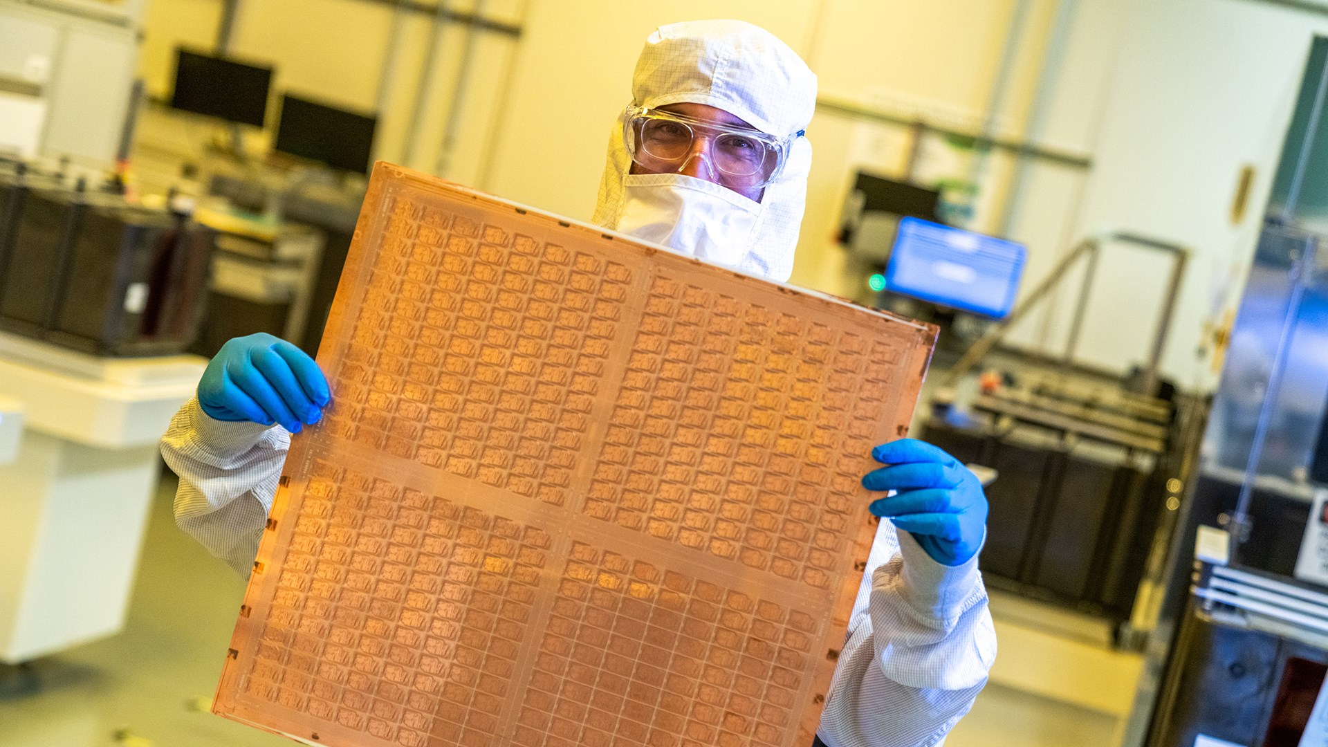
Glass substrates are produced from materials such as borosilicate, quartz and fused silica and offer superior advantages over traditional organic materials. These materials provide exceptional flatness, dimensional stability and superior thermal and mechanical durability. Consequently, these advantages make them more reliable in application areas such as data center processors.
AMD patented its solutions
See Full Size
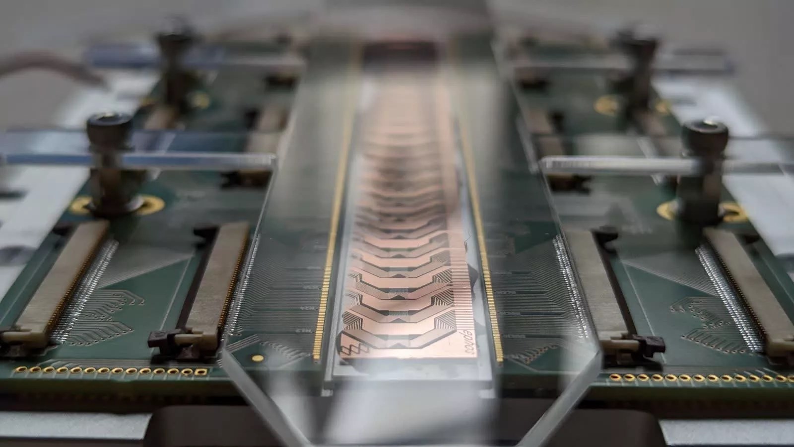
Redistribution layers Redistribution Layers (RDL) also play a critical role in advanced chip packaging. These layers transfer signals and energy between the chip and external components through high-density connections. Unlike glass substrates, these will continue to use organic dielectric materials and copper; but this time they will be built on one side of the glass wafer and will require a new manufacturing method.
The patent also provides strong, gap-free connections copper based bonding It also describes a new method for bonding multiple glass substrates using (instead of traditional solder strokes). This makes the connections more durable and eliminates the need for additional filling materials.
AMD’s patent reveals that glass substrates offer significant advantages in data center processors, such as thermal management, mechanical durability and improved signal management. However, it is stated that this technology can also be applied in various areas that require intensive connection, such as mobile devices, computer systems and even advanced sensors.
This news our mobile application Download using
You can read it whenever you want (even offline):


